Doping Chips at Home
I’m using a homemade tube furnace and commercial jewelry oven to dope some semiconductor devices with a home-brew SOD Dopant. My process is based on Jeri Ellsworth and Sam Zeloof’s chip doping work, and my SOD recipe is based on ProjectsinFlight's.

I've succesfully doped PN junctions to make diodes and photovoltaics. I've also made MOSFETS with poor characteristics.
I modeled my homemade tube furnace using the fourier heat equation here.
Failed MOSFETs and Diodes
IV Curve of Home Doped Diode

IV Curve of Home Doped Mosfet (Gate Voltage Sweep)
The above video is the best IV curve I've generated so far. The gate dielectric broke down as I did the voltage sweep, however, so I don't count this as a functional MOSFET.
MOSFET Fab Process Overview
I use a thermal oxide and thermal diffusion process to grow SiO2 layers on top of P <100> wafers and dope N-type regions in said wafers. Below is a quick overview of each fabrication step with key information.
Step 1: Grow Thermal Oxide Layer
2: HF Etch the Oxide Layer
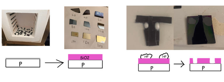
1.1 P type silicon wafers with orientation 100 are cooked for 3-6 hours at 1000 celsius to grow a roughly 500 nm oxide (Fig 1). Oxide thickness can be estimated based on the color/thin film intereference on the wafer (Fig 2).
1.2 I've experimented with blowing steam into the furnace to speed up oxidation, but my wet oxides are more suceptible to contamination.
Fig 1
Fig 2
Fig 3
Fig 4
2.1 The silicon dioxide layer is etched with armor etch glass etchant HF cream (Fig 3). After 2-5 minutes the oxide layer is completely removed in etched spots
(Fig 4).

3: Grow Passervation oxide
3.1 A thin passervation layer (~10 nm) is grown at 1000 C for ~ 1 minute to make the etched regions of the silicon wafer more hydrophillic.
3.2 The passervation layer needs to be thin enough that the liquid dopant will still difuse into the silicon. Without the passervation layer the liquid dopant won't evenly coat the chip.
Fig 5
Fig 6
4: Coat Chip in Liquid Dopant
4.1 The chip is coated in a Phosphoric Acid and TEOS solution, spun around on a computer fan to create an even film, and heated at 200 C for 15 minutes. This grows a Phosphoric Acid glass dopant on the surface of the chip.
4.2 The spin on dopant solution is a 1:1:0.5:4 volume mix of water, TEOS, Phosphoric Acid, and Ethyl Alchol from ProjectsInFlight. A reflux aparratus is used to boil the solution for 1 Hour, catalyzing the Sol Gel reaction without affecting the mixture ratio (Fig 6).
5: Thermal Diffusion
6: HF Etch

5.1 A home-made tube furnace (Fig 7, 8) is used to diffuse N-type regions into the P substrate at 1000 C for 1 hour.
Fig 7

Fig 8
6.1 The oxide on the chip surface is completely etched away using HF.
7: Grow Gate Oxide
8: Make Epoxy Contacts

7.1 The chip is heated at 1000 C for 30 minutes to grow a red to blue gate oxide (~100 nm).
7.2 The most sensitive part of this process is the gate oxide. A thinner gate oxide will lower the gate threshold of the device, but is also more susceptible to shorts and dielectric breakdown.
7.3 My gate oxides tend to break down around 25 Volts, at which point the oxide stops insulating and a gate source current develops. This destroys the device as the gate needs a strong dielectric to function.
8.1 The oxide over the N channels is etched away and silver epoxy is applied to the Source, Gate, Drain, and Substrate to create ohmic contacts. Resistor leads are used with the epoxy to make the MOSFET bread board compatible.
8.2 The epoxy contact on the gate oxide should cover a large area to increase the capacitance of the gate.